
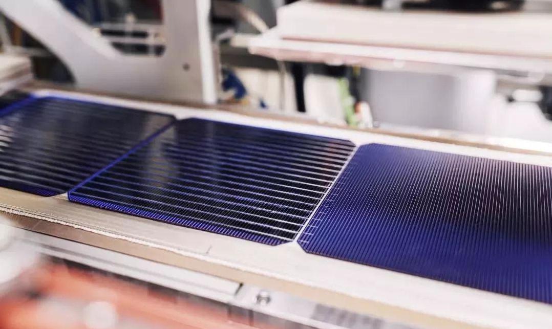
high Technology Amorphous Silicon Cells The main factors affecting the conversion efficiency and stability
Since the amorphous silicon cells structure is a random network structure with long-range disorder, it has a strong scattering effect on the carriers, resulting in the carriers cannot be effectively collected.
In order to increase the amorphous silicon solar cell conversion efficiency and stability, generally do not take a single crystal silicon solar cell of p-n structures.
This is because the Fermi energy level shift of lightly doped amorphous silicon is small. If both sides are lightly doped or one side is lightly doped and the other side is heavily doped, the band bending will be smaller and the open circuit voltage of the cell will be affected.
Restriction: If the heavily doped p+ and n+ materials are directly used to form a p+ -n+ junction, the cell performance will be poor due to the high density of defect states in the heavily doped amorphous silicon material and the low lifetime of minority carriers. Therefore, an undoped amorphous silicon layer (i layer) is usually deposited in the two heavily doped layers as the active collector area, that is, the p-i-n structure.
The photo-generated carriers of amorphous silicon solar cells are mainly generated in the undoped i-layer, which is different from the carriers of crystalline silicon solar cells which move mainly due to diffusion. In amorphous silicon solar cells, the photo-generated carriers are due to the diffusion length.
Drifting mainly depends on the electric field in the cell. When the amorphous silicon cells adopts the pin structure, the cell can work under light, but due to the light-induced degradation effect, the cell performance is unstable, and the cell conversion efficiency gradually declines with the light time, so the structure and process of the cell need to be further optimization.

Factors affecting the performance of amorphous silicon cells
The main factors affecting the conversion efficiency and stability of amorphous silicon cells are: transparent conductive film, window layer properties (including window layer optical band gap width, window layer conductivity and doping concentration, window layer activation energy, window layer light transmission Overrate), the interface state between the layers (interface defect state density) and energy gap matching, the thickness of each layer (especially the thickness of the i layer), and the solar cell structure.
The structure of amorphous silicon thin-film cells generally takes the form of stacked or integrated or structured heterojunctions.
Amorphous silicon cells has simple production process, low temperature and low energy consumption, and its market share is increasing year by year. Currently, more than half of thin film solar cell companies use amorphous silicon thin film technology . It is expected that in a few years, amorphous silicon thin films will occupy a major share of thin film solar cells in the future. However, low photoelectric conversion efficiency and light-induced degradation are the two main problems of current amorphous silicon thin-film cells. In order to improve efficiency and stability, people need to strengthen exploration in new device structures, new materials, new processes and new technologies.
For example, in terms of cell structure, laminated and integrated types are adopted; in terms of transparent conductive film, a transparent conductive film that not only has low resistivity but also has the effects of blocking ion pollution, increasing incident light absorption and anti-radiation effects, replaces the current ITO and ZnO. , ZnO#Al and other conductive films.
In terms of window layer materials, explore new window layer materials with wide optical band gap and low resistance materials, such as amorphous silicon carbon, amorphous silicon oxide, microcrystalline silicon, microcrystalline silicon carbon, etc.
In terms of amorphous silicon thin film preparation technology, RF-PECVD, ultra-high vacuum PECVD technology, very high frequency (VHF) PECVD technology and microwave PECVD technology can be improved to extend the photon life of the thin film, improve the carrier transport capacity and the electron of the thin film. Performance and stability; in interface treatment, hydrogen passivation technology and insertion of buffer layers can be used to reduce interface recombination loss and increase cell short-circuit current and open-circuit voltage.
Although the current low efficiency and unstable performance are the main obstacles hindering the large-scale industrial production of amorphous silicon thin-film solar cells, various technologies for optimizing amorphous silicon thin-film solar cells are still feasible. With the further development of science and technology, amorphous silicon Thin-film solar cells will be used on a large scale.