
TSMC New Factory In Japan, Taiwan OEM Taiwan Accumulation Circuit Manufacturing Company (TSMC) and Sony Semiconductor Solutions, a subsidiary of Sony Group, announced on the 9th that they would set up a semiconductor OEM subsidiary in Kumamoto Prefecture, Japan.

TSMC New Factory In Japan start construction of a new factory in 2022, striving to invest before the end of 2024. Production. The initial investment in equipment is expected to be about $70 billion, and Sony’s investment is about $5 billion, winning less than 20% of the shares.
The new factory will be built in Kikuyo Town, Kumamoto Prefecture, Japan, and can create about 1500 jobs for cutting-edge technical talents. This is the first time that TSMC has set up a production base in Japan.
The subsidiary is called JASM. TSMC New Factory In Japan will put into operation for semiconductors with a process of 22 nanometers (1 nanometer of 1 billionth of meters) and 28 nanometers.
Sony said that the partnership with TSMC new factory is conducive to the stable procurement of semiconductors, which is of great significance.
The Japanese government regards ensuring semiconductors as an important topic of economic security and actively attracts investment, and intends to provide about half of the cost of assistance. TSMC and Sony said that “discussion is under way on receiving strong assistance from the Japanese government”. TSMC New Factory In Japan is so important.
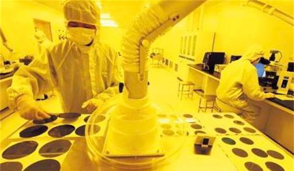
According to the report, TSMC, with Taiwan as its headquarters, has world-class technical strength in semiconductor manufacturing, and has also achieved mass production of high-performance 5nm products for smartphones and so on which help TSMC New Factory advanced Technology.
TSMC has also built a semiconductor manufacturing plant in Arizona, western United States, producing 2 million 5nm semiconductors per month from the first quarter of 2024.
Bank of China Securities: The high performance growth of ASML, TSMC and other performance indicates that the industry will maintain a high boom.
Bank of China Securities pointed out that ASML’s third-quarter performance exceeded expectations, and new orders rebounded sharply.
TSMC raised its annual revenue growth rate, and SMIC International also significantly increased its revenue guidelines for the third quarter.
Wafer OEMs expanded capital expenditure, and shipments of semiconductor equipment in North America continued to grow at a high year-on-year basis. The bidding speed of local wafer factories has been accelerated, and domestic manufacturers have won the bid for a batch of process equipment and TSMC New Factory will help increasing production.
The semiconductor equipment industry will maintain a high boom:
1) ASML monopolizes more than 90% of the global lithography machine, and the lithography machine is the core equipment of the wafer production line, so the delivery and order are representative.
2) TSMC and SMIC’s performance exceed expectations, reflecting the continued strong downstream demand.
Taiwan Semiconductor Manufacturing Company (TSMC) has made important breakthroughs in the research and development of 2nm semiconductor manufacturing nodes. This breakthrough report has surfaced in the Taiwanese media and has been picked up by the Oriental media.
TSMC, which is responsible for providing processors and other chips to various companies around the world, is also expected to enter the trial production stage of the process in mid-2023 and start mass production in a year.
TSMC 2nm node will mark a major leap in current chip manufacturing technology specially with TSMC new factory.
At present, TSMC latest manufacturing node is its first generation of 5nm process, which will be used to build processors for Apple flagship smartphones in 2020. In layman’s terms, “node” refers to the size measurement of the transistor “fin”. Today’s processors consist of billions of such fins, which enable computing to achieve unparalleled complexity and reduce costs and performance also TSMC new factory will affect that in future.
Contrary to “finFET”, this term is used to describe the transistor design of products manufactured by TSMC and the Samsung OEM department of Chaebol Samsung Electronics in South Korea, while TSMC 2nm process will adopt differential transistor design. This design is called a multi-bridge channel field effect (MBCFET) transistor, which complements the previous FinFET design.

FinFET design involves three basic elements. They are source poles, gates and drain poles. Electrons flow from the source pole to grains, and the gate regulates this flow. FinFET’s previous design involved manufacturing source and drain electrodes only on horizontal axis, that is, they were leveled with the chip discussed.
FinFET’s innovative method increases the source and drain poles in three dimensions (i.e. vertical), so it allows more electrons to pass through the gate, thus reducing leakage and working voltage.
TSMC’s decision to design MBCFET for its transistors was not the first time that the wafer OEM made this decision. Samsung announced the design of its 3nm manufacturing process in April last year. The company’s MBCFET design is an improvement on the GAAFET transistor jointly developed and launched with IBM in 2017.
Compared with GAAFET, Samsung MBCFET uses nanowires and drain poles (channels). This increases the surface area that can be used for conduction and, more importantly, allows designers to add more gates to transistors without increasing the transverse surface area.
There are also unsourced statements in the media, which also implies that TSMC expects the yield of its 20nm process nodes to reach an astonishing 90% in 2023. If this happens, the wafer factory will improve its manufacturing process well and easily turn to mass production and mass production by 2024. Samsung said in the release of MBCFET that it expects 3nm transistors to consume 30% less power and 45% less than the 7nm design, respectively, and improve performance by 30% and waiting 2022 TSMC new factory.
It is uncertain whether TSMC 2nm process will provide similar improvements, but once the design parameters of the process are determined, we should find more information. Based on IBM and Samsung’s 5nm GAAFET design, which can squeeze amazing 300 billion transistors in a surface area of 50mm2, the sky does seem to be the limit of TSMC.